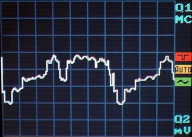
LS020 176 x 128 8 bit (строчные импульсы 15 кГц) Развертка 10 мкс/дел
AVI файлы видеосигнала (строчные импульсы 15 кГц) Развертка 10 мкс/дел
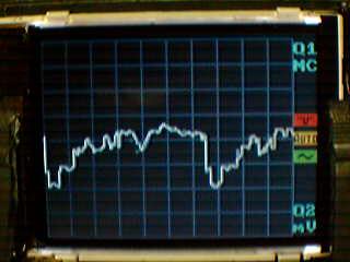
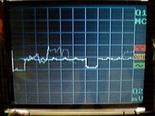
Схема подключения дисплея LS020 к Atmega 644
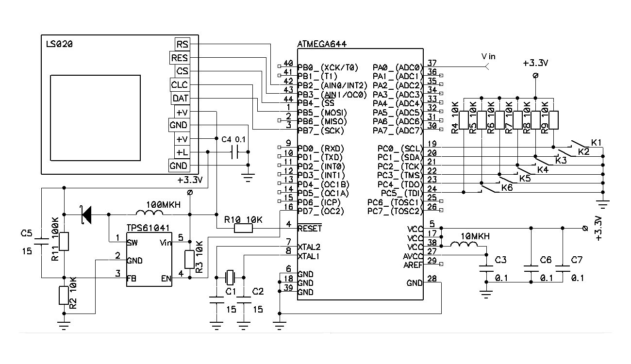
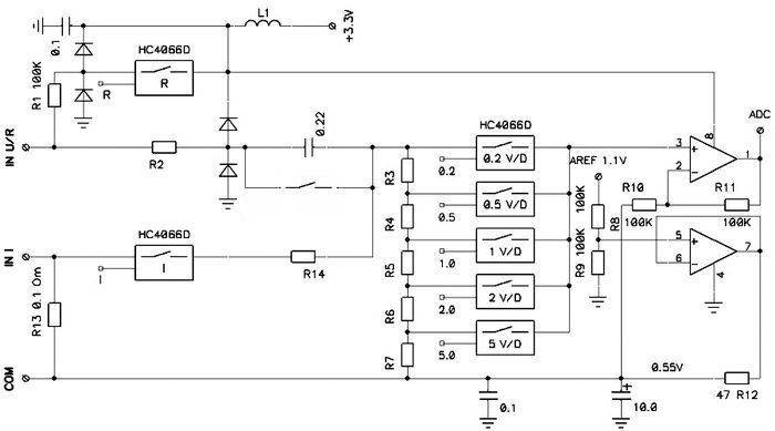
Схема аналоговой части:
Программа (asm)
Инициализация АЦП ATmega 644
adcinit:
; REFS1=1 REFS0=0 (Internal 1.1V Voltage Reference with external capacitor at AREF pin), ADLAR=1(Left), MUX = 0
ldi temp, (1<<REFS1) | (1<<ADLAR)
sts ADMUX, temp
; ADEN=1(ADCenable), ADSC=1(Start), ADATE=1(Auto Trigger Enable) ADPS: /64
ldi temp,(1<<ADEN) | (1<<ADSC) | (1<<ADATE) | (1<<ADPS2) | (1<<ADPS1) | (0 <<ADPS0)
sts ADCSRA, temp
ldi temp, 0b01000000 ; Free Running mode
sts ADCSRB, temp
ret
Регистры Analog-to-digital Converter ATmega644
ADMUX – ADC Multiplexer Selection Register
• Bit 7:6 – REFS1:0: Reference Selection Bits
These bits select the voltage reference for the ADC, as shown in Table 21-3. If these bits are changed during a conversion, the change will not go in effect until this conversion is complete (ADIF in ADCSRA is set). The internal voltage reference options may not be used if an external reference voltage is being applied to the AREF pin. Note: If 10x og 200x gain is selected, only 2.56V should be used as Internal Voltage Reference.
• Bit 5 – ADLAR: ADC Left Adjust Result The ADLAR bit affects the presentation of the ADC conversion result in the ADC Data Register. Write one to ADLAR to left adjust the result. Otherwise, the result is right adjusted. Changing the ADLAR bit will affect the ADC Data Register immediately, regardless of any ongoing conversions.
• Bits 4:0 – MUX4:0: Analog Channel and Gain Selection Bits The value of these bits selects which combination of analog inputs are connected to the ADC. These bits also select the gain for the differential channels. If these bits are changed during a conversion, the change will not go in effect until this conversion is complete (ADIF in ADCSRA is set).
| 7 | 6 | 5 | 4 | 3 | 2 | 1 | 0 |
| REFS1 | REFS0 | ADLAR | MUX4 | MUX3 | MUX2 | MUX1 | MUX0 |
• Bit 7:6 – REFS1:0: Reference Selection Bits
These bits select the voltage reference for the ADC, as shown in Table 21-3. If these bits are changed during a conversion, the change will not go in effect until this conversion is complete (ADIF in ADCSRA is set). The internal voltage reference options may not be used if an external reference voltage is being applied to the AREF pin. Note: If 10x og 200x gain is selected, only 2.56V should be used as Internal Voltage Reference.
• Bit 5 – ADLAR: ADC Left Adjust Result The ADLAR bit affects the presentation of the ADC conversion result in the ADC Data Register. Write one to ADLAR to left adjust the result. Otherwise, the result is right adjusted. Changing the ADLAR bit will affect the ADC Data Register immediately, regardless of any ongoing conversions.
• Bits 4:0 – MUX4:0: Analog Channel and Gain Selection Bits The value of these bits selects which combination of analog inputs are connected to the ADC. These bits also select the gain for the differential channels. If these bits are changed during a conversion, the change will not go in effect until this conversion is complete (ADIF in ADCSRA is set).
ADCSRA – ADC Control and Status Register A
• Bit 7 – ADEN: ADC Enable Writing this bit to one enables the ADC. By writing it to zero, the ADC is turned off. Turning the ADC off while a conversion is in progress, will terminate this conversion.
• Bit 6 – ADSC: ADC Start Conversion In Single Conversion mode, write this bit to one to start each conversion. In Free Running Mode, write this bit to one to start the first conversion. The first conversion after ADSC has been written after the ADC has been enabled, or if ADSC is written at the same time as the ADC is enabled, will take 25 ADC clock cycles instead of the normal 13. This first conversion performs initialization of the ADC. ADSC will read as one as long as a conversion is in progress. When the conversion is complete, it returns to zero. Writing zero to this bit has no effect.
• Bit 5 – ADATE: ADC Auto Trigger Enable When this bit is written to one, Auto Triggering of the ADC is enabled. The ADC will start a conversion on a positive edge of the selected trigger signal. The trigger source is selected by setting the ADC Trigger Select bits, ADTS in ADCSRB.
• Bit 4 – ADIF: ADC Interrupt Flag This bit is set when an ADC conversion completes and the Data Registers are updated. The ADC Conversion Complete Interrupt is executed if the ADIE bit and the I-bit in SREG are set. ADIF is cleared by hardware when executing the corresponding interrupt handling vector. Alternatively, ADIF is cleared by writing a logical one to the flag. Beware that if doing a Read-Modify- Write on ADCSRA, a pending interrupt can be disabled. This also applies if the SBI and CBI instructions are used.
• Bit 3 – ADIE: ADC Interrupt Enable When this bit is written to one and the I-bit in SREG is set, the ADC Conversion Complete Interrupt is activated.
• Bits 2:0 – ADPS2:0: ADC Prescaler Select Bits These bits determine the division factor between the XTAL frequency and the input clock to the ADC.
| 7 | 6 | 5 | 4 | 3 | 2 | 1 | 0 |
| ADEN | ADSC | ADATE | ADIF | ADIE | ADPS2 | ADPS1 | ADPS0 |
• Bit 7 – ADEN: ADC Enable Writing this bit to one enables the ADC. By writing it to zero, the ADC is turned off. Turning the ADC off while a conversion is in progress, will terminate this conversion.
• Bit 6 – ADSC: ADC Start Conversion In Single Conversion mode, write this bit to one to start each conversion. In Free Running Mode, write this bit to one to start the first conversion. The first conversion after ADSC has been written after the ADC has been enabled, or if ADSC is written at the same time as the ADC is enabled, will take 25 ADC clock cycles instead of the normal 13. This first conversion performs initialization of the ADC. ADSC will read as one as long as a conversion is in progress. When the conversion is complete, it returns to zero. Writing zero to this bit has no effect.
• Bit 5 – ADATE: ADC Auto Trigger Enable When this bit is written to one, Auto Triggering of the ADC is enabled. The ADC will start a conversion on a positive edge of the selected trigger signal. The trigger source is selected by setting the ADC Trigger Select bits, ADTS in ADCSRB.
• Bit 4 – ADIF: ADC Interrupt Flag This bit is set when an ADC conversion completes and the Data Registers are updated. The ADC Conversion Complete Interrupt is executed if the ADIE bit and the I-bit in SREG are set. ADIF is cleared by hardware when executing the corresponding interrupt handling vector. Alternatively, ADIF is cleared by writing a logical one to the flag. Beware that if doing a Read-Modify- Write on ADCSRA, a pending interrupt can be disabled. This also applies if the SBI and CBI instructions are used.
• Bit 3 – ADIE: ADC Interrupt Enable When this bit is written to one and the I-bit in SREG is set, the ADC Conversion Complete Interrupt is activated.
• Bits 2:0 – ADPS2:0: ADC Prescaler Select Bits These bits determine the division factor between the XTAL frequency and the input clock to the ADC.
ADCSRB – ADC Control and Status Register B
• Bit 7, 5:3 – Res: Reserved Bits
• Bit 2:0 – ADTS2:0: ADC Auto Trigger Source If ADATE in ADCSRA is written to one, the value of these bits selects which source will trigger an ADC conversion. If ADATE is cleared, the ADTS[2:0] settings will have no effect. A conversion will be triggered by the rising edge of the selected Interrupt Flag. Note that switching from a trigger source that is cleared to a trigger source that is set, will generate a positive edge on the trigger signal. If ADEN in ADCSRA is set, this will start a conversion. Switching to Free Running mode (ADTS[2:0]=0) will not cause a trigger event, even if the ADC Interrupt Flag is set.
| 7 | 6 | 5 | 4 | 3 | 2 | 1 | 0 |
| - | ACME | - | - | - | ADTS2 | ADTS1 | ADTS0 |
• Bit 7, 5:3 – Res: Reserved Bits
• Bit 2:0 – ADTS2:0: ADC Auto Trigger Source If ADATE in ADCSRA is written to one, the value of these bits selects which source will trigger an ADC conversion. If ADATE is cleared, the ADTS[2:0] settings will have no effect. A conversion will be triggered by the rising edge of the selected Interrupt Flag. Note that switching from a trigger source that is cleared to a trigger source that is set, will generate a positive edge on the trigger signal. If ADEN in ADCSRA is set, this will start a conversion. Switching to Free Running mode (ADTS[2:0]=0) will not cause a trigger event, even if the ADC Interrupt Flag is set.
DIDR0 – Digital Input Disable Register 0
• Bit 7..0 – ADC7D..ADC0D: ADC7..0 Digital Input Disable When this bit is written logic one, the digital input buffer on the corresponding ADC pin is disabled. The corresponding PIN Register bit will always read as zero when this bit is set. When an analog signal is applied to the ADC7..0 pin and the digital input from this pin is not needed, this bit should be written logic one to reduce power consumption in the digital input buffer.
• Bit 7..0 – ADC7D..ADC0D: ADC7..0 Digital Input Disable When this bit is written logic one, the digital input buffer on the corresponding ADC pin is disabled. The corresponding PIN Register bit will always read as zero when this bit is set. When an analog signal is applied to the ADC7..0 pin and the digital input from this pin is not needed, this bit should be written logic one to reduce power consumption in the digital input buffer.
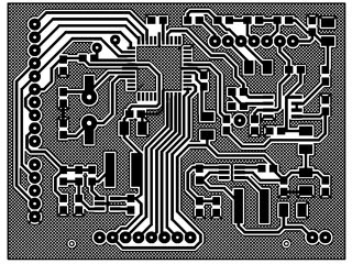
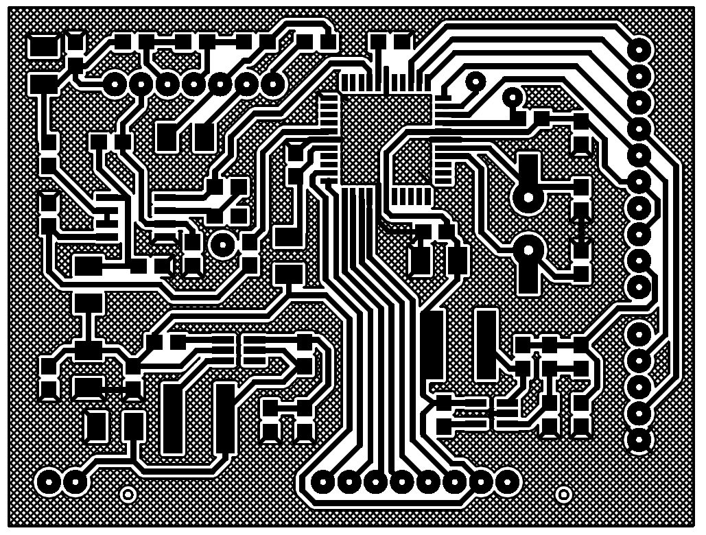
Разводка печатной платы